In recent years, the application of PD fast charging technology in communication terminal products has gradually become popular, and the market demand has continued to expand. Major machine manufacturers have successively launched products that apply PD fast charging technology. In the current global core shortage environment, the PD fast charging products on the market have many shortcomings in terms of product functions, product quality, and delivery deadlines.
In view of the fact that traditional technical solutions on the market cannot meet the demand for high power density, GaN applications have market pain points such as high overall cost, complex application debugging, EMI resolution, high reliability requirements, and difficulty in ensuring stable delivery. Universal Semiconductor has launched the industry's first highly integrated PD power chip G1661D that meets the full voltage requirements of PD fast charging with industry-leading technology research and development and power application design capabilities. It adopts the unique patented technology of high-voltage process pioneered by the global semiconductor industry, and through high-efficiency super-junction power device drive control technology and high-power-density package integration, it achieves high efficiency, high reliability, high integration, and can meet customers' long-term And stable demand delivery.
For 25-33W PD fast charging applications, Global Semiconductor designed and mass-produced: G1661D+G3617CF complete design scheme, primary power chip G1661D, built-in 650V low on-resistance super junction MOS, industry-leading high-voltage process, VCC power supply support Above 80V, it meets the requirements of PD fast charge and full voltage output. The main chip adopts 90KHz operating frequency. Through frequency hopping and green energy-saving mode, the standby loss of the product is reduced, and the CCM&QR working mode is supported, which improves the efficiency of the power supply and realizes the miniaturization of the power supply. At the same time, it also has complete protection functions such as cycle-by-cycle over-current detection, output over-voltage, over-current, and over-temperature. It adopts the industry’s innovative DFN6*5-10L package to provide stable and reliable high heat dissipation performance to meet customers’ high requirements. Demand for quality power solutions.
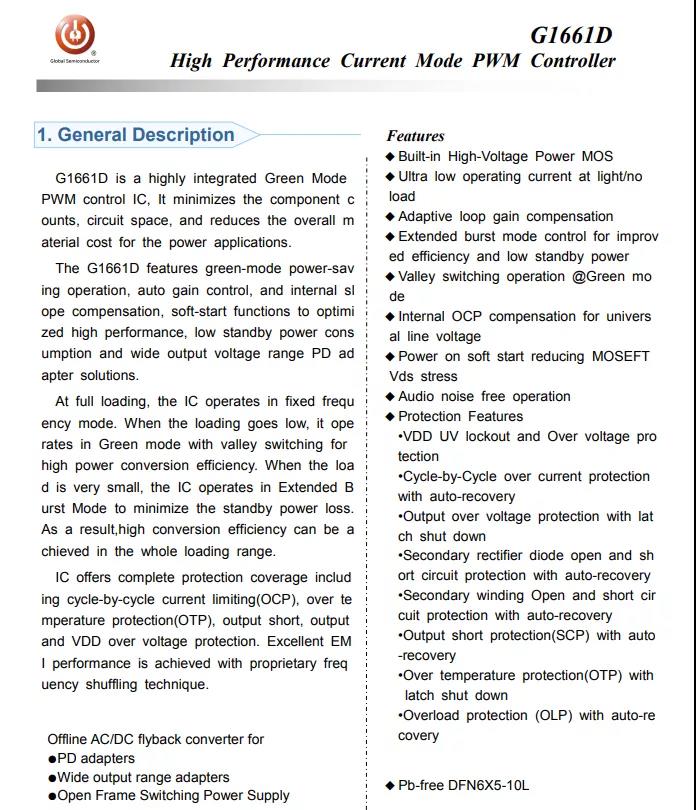
环球半导体G1661D详细资料。
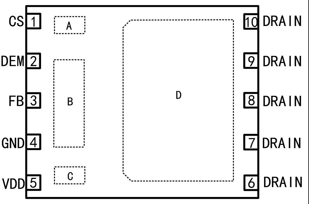
环球半导体G1661D封装图。
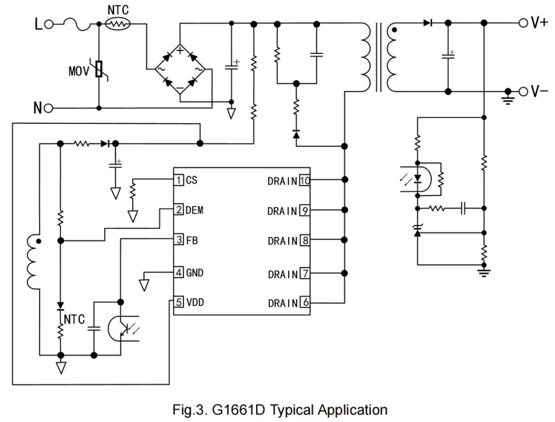
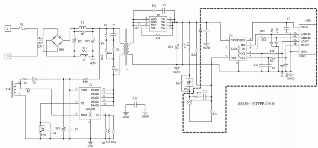
方案原理图。
次级同步整流采用环球半导体的G3617CF,内置100V 10mR MOS,SOP8封装,环球半导体已批量的G3667xF(60V)、G3687xF(80V)、G3617xF(100V)三个系列同步整流芯片,采用行业领先的高压BCD工艺,支持CCM、DCM、QR模式,有效抑制CCM模式下VDS尖峰问题的同时可以获得最佳的转换效率,专利技术的VCC供电结构和开启关断检测电路可以获得极简的外围电路设计。
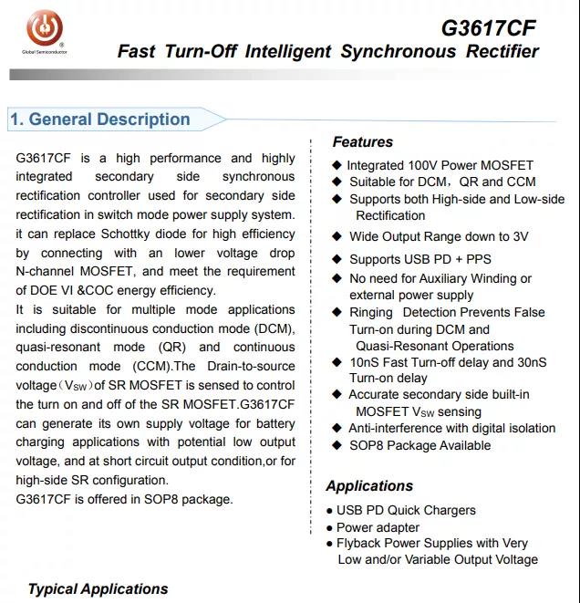
环球半导体G3617CF详细资料。
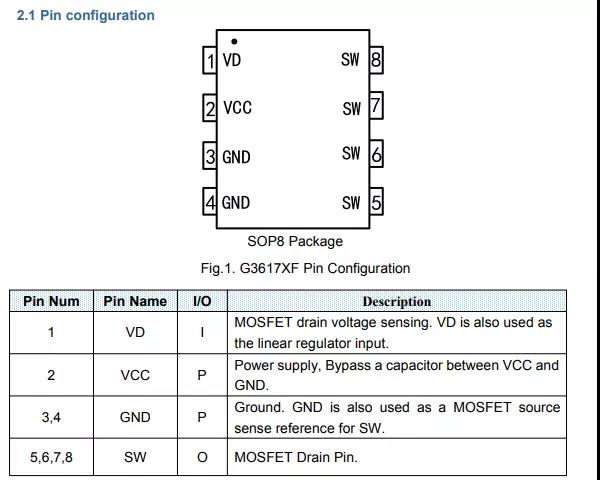
环球半导体G3617CF封装及引脚定义。
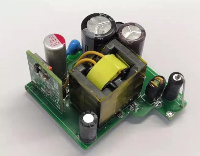
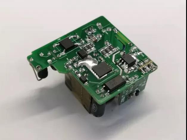
30W PD快充原理图
30W PD能效测试数据

30W PD温度测试数据(装壳测试)
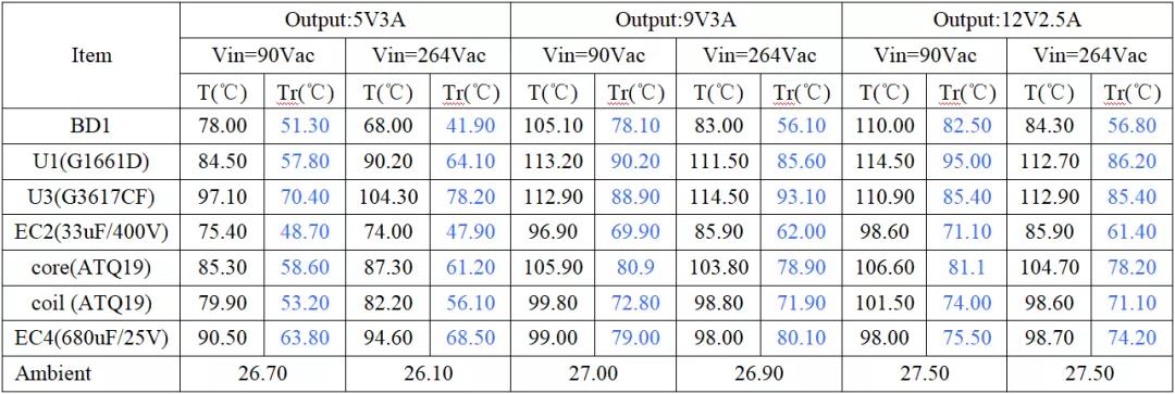
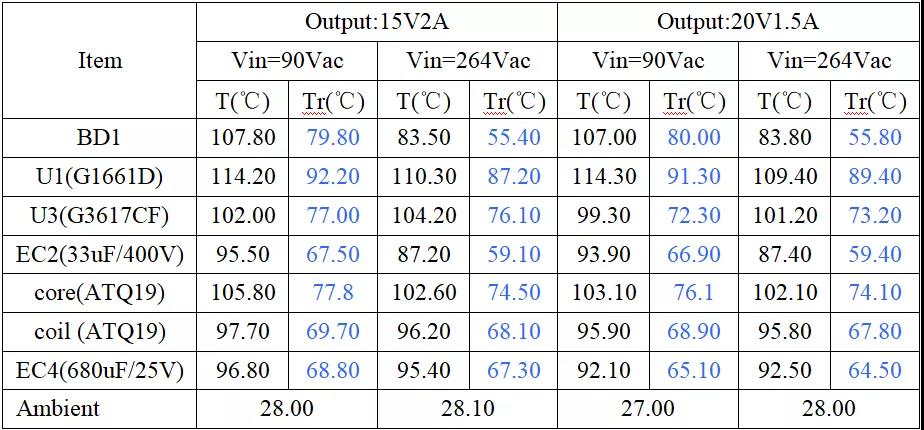
Summarize:
Global Semiconductor’s G1661D power management chip is based on advanced high-voltage manufacturing processes, which perfectly simplifies the peripheral circuit design. Through efficient super-junction power device drive control technology and high-power-density packaging structure, it can solve customers’ high-power PD power solutions. Performance, high reliability, easy EMC processing and continuous delivery requirements.
GlobalSemi was founded in 2012. The core technical team comes from well-known semiconductor design companies at home and abroad, and all have more than 18 years of work experience in power management IC R&D and system applications. The company has established a joint R&D laboratory with the School of Microelectronics, Xidian University and South China University of Technology, and has achieved a number of technological innovations. The company combines advanced power management architecture design, semiconductor technology, and packaging technology to successfully develop multiple series of high-performance, high-power-density power chip products. The product technology is at the forefront of international power IC design. The company has long focused on the R&D and design of high-quality power management ICs. Products are widely used in: mobile communication equipment, white goods, motor power supplies, industrial power supplies, medical equipment, 5G smart devices, and home power management systems.
Global Semiconductor will continue to focus on customer needs, adhere to technological innovation, lead new technologies, high-density packaging technology, and persevere in reducing overall costs for users as its operating principles, and will soon launch a fast charging design with an integrated power of 45~65W Solution chip.